About
The vision of HETPil is to demonstrate the first fully monolithically integrated ultra narrow linewidth frequency agile laser, based on recently emerged hybrid opto-electro-mechanical systems. This laser combines piezo-electrical MEMS technology monolithically integrated on ultra low loss silicon nitride integrated photonic circuits, and active lasers integrated using tranfer printing. This integrated laser exhibits distincts and previously distinct properties that could not be united in a single device: ultra narrow linewidth and unprecedentedly fast MHz bandwidth tuning, that is ultra low power, hysteris free, and fully compatible with wafer scale large volume manufacturing. These properties lie at the heart of two novel applications for which integrated lasers are required: FCMW LiDAR for autonomous driving and driver assistance, and 5/6G, which are explored as applications in this project. Taken together our project lays the foundation to a new hybrid, integrated laser based on opto-electro-mechanical technology.
Project
Highly coherent – that is narrow linewidth – laser sources are at the heart of numerous applications: ranging from terabit per second coherent communication, LiDAR for autonomous driving or driver assistance, to fibre sensing or optical atomic clocks. Yet, in contrast to MEMS sensors, or electroni circuits, the manufacturing of narrow linewidth lasers is not suitable for high volume; fiber lasers, the workhorse for narrow linewidth, rely on bulk fibre based optical components assembled manually. In recent years, triggered by new applications in particular in FMCW LiDAR, the demand for integrated lasers that combine the coherence of a narrow linewidth fibre laser with high frequency agility and fast tuning, and can be manufactured wafer-scale in large volume at low cost has become a technological bottleneck.
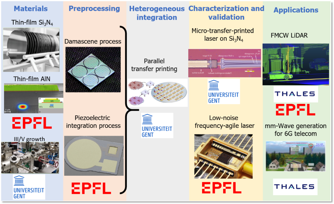
Here we overcome these challenges and will demonstrate for the first time a mass manufacturable, compact, wafer-scale narrow linewidth laser with unprecedentedly agile tuning and precise laser tuning. To achieve this novel technology, we will employ recent findings on a hybrid electro-opto—mechanical integrated laser obtained in the FET Proactive project “Hybrid Optomechanical Technologies.” To combine the conflicting properties of ultrahigh coherence and fast and precise tuning, we will combine sub-micron piezo-electrical actuators that rely on AlN – a proven MEMS technology – that combine an electrical and mechanical engineered degrees of freedom with silicon nitride ultra-low loss integrated photonic circuits. The combined hybrid opto-electro-mechanical device exhibits unique performance characteristics in terms of linewidth and frequency agility not attained anywhere to date, making them ideal sources for LiDAR.
FMCW LiDAR is a next generation perception technology enabled by narrow linewidth highly tunable lasers that has major advantages compared to the currently used time of flight LiDAR: it is eye-safe and crucially can give both velocity and distance information in the same pixel – massively simplifying the object classification. FMCW can even operate in glaring sunlight, is immune to crosstalk from other sensors, and is ideally suited for long-range detection as required for autonomous driver assistance. It is, however, compounded by the very stringent requirements: it requires exceptionally narrow linewidth, highly linear tuning of the laser, and above all, this technology, being applied to mass markets, is required to be manufactured in large volumes at low cost.
Ultra-stable, fast and linearly tunable lasers are also key enabling technology for reconfigurable, ultra-broadband wireless transmitters for future wireless communications. Using the unoccupied mmWave band above 100 GHz requires low-cost yet very high performance tunable laser systems and high-bandwidth photoreceivers to cope with the requirements of dense mesh area coverage imposed by the significant atmospheric absorption at these frequencies.
In this project, we will manufacture such hybrid integrated lasers using volume-manufacturing compatible techniques only – using both monolithic and transfer printing techniques – improve their tuning and linewidth further, and test them in a relevant application scenario for FMCW LiDAR and validate the combination of NOEMS technologies and integrated photonics devices for use in optical communication by demonstration of tight phase locking using the novel actuator technology.
Technology
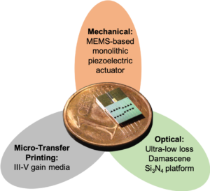
Nano-electro-mechanical concept of the HetPIL laser systems is free-fold. We combine three degrees of freedom: optical, mechanical and electrical.
We will combine sub-micron piezo-electrical actuators that rely on AlN – a proven MEMS technology – that combine an electrical and mechanical engineered degrees of freedom with silicon nitride ultra-low loss integrated photonic circuits. The combined hybrid opto-electro-mechanical device exhibits unique performance characteristics in terms of linewidth and frequency agility not attained anywhere to date, making them ideal sources for LiDAR.
Optical: low-loss silicon nitride
The low-loss silicon nitride platform stands as a pivotal foundation within the HETPIL project. Its exceptional properties, including high thermal stability, low optical losses, and precise control over material dimensions, serve as a cornerstone for enhancing the efficiency and effectiveness of thermophotovoltaic energy conversion systems. This platform enables the manipulation of light at the nanoscale, allowing for the creation of highly efficient photon management strategies, thereby paving the way for significant advancements in energy harvesting and conversion technologies within the HETPIL.
Mechanical: MEMS actuators
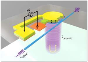
The key component of this technology is a sub-micron electro-optomechanical transducer that is composed of a piezoelectric thin film and matched electrodes that are monolithically integrated on a silicon nitride photonic integrated circuit chip. This actuator enables control over the phase/frequency and amplitude response of the photonic waveguides and microresonators with extremely low power consumption. The frequency agility envisaged for the HetPIL lasers crucially relies on tuning actuators with response times of the order of 1 ns or less, corresponding to actuation bandwidths of the order of 1 GHz or more. To this end, we will use advanced piezoelectric actuators that can be co-integrated with low-loss silicon nitride strip waveguides and that allow highly efficient high-speed phase tuning via the stress-optical effect.
Electrical: micro-transfer printing

We propose micro-transferprinting as the technique that allows to overcome the limits of classic wafer bonding. The concept of transfer-printing. Firstly, a device is patterned on the source substrate which can be e.g. a III-V wafer. Then, the photoresist is used to create tethers, i.e. to ‘anchor’ the device (alternatively, silicon nitride, silicon oxide, or the device layer itself can be used to make tethers). In the next step, the so-called release layer underneath the device is etched, so we are left we a free-standing device held by tethers. Finally, the actual micro-transfer printing is done: an elastomeric stamp is used to pick up the device (breaking the tethers) and print it on the target wafer (which will be the silicon nitride interposer in this project). Devices can be transferred with a 3σ placement accuracy of ±0.3 µm on wafer-scale equipment for small arrays or single devices. Pattern recognition is used for accurate placement. As the source and target wafer are processed separately, high-quality materials and standard, well-developed process flows can be used for both the source and target.
Applications

mm-wave optical local oscillator generation for 5/6G future networks
The mm-wave local oscillator (LO) demonstrator will be built around the HetPIL dual laser photonic chip, as described in the figure below. An in-depth characterization of the individual lasers’ FM transfer functions will enable the design and realisation of optimized loop filter electronic circuits for mutual phase locking of the two lasers. The phase noise of the resulting beatnote will be measured and characterized. Then, to truly assess the potential of the HetPIL technology for future wireless networks, we will implement a back-to-back transmission link, using our OPLL-based LO to carry an analogue radio-over-fiber OFDM signal. The Error Vector Magnitude (EVM) of the recorded constellations will be evaluated for various complex formats (16, 64, 256QAM), and confronted to 5G requirements The measurements will be carried out without post-processing compensation, in order to favor real time processing capability.
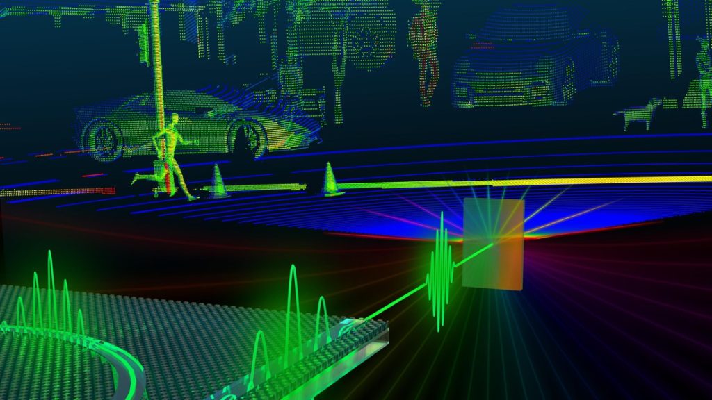
FMCW LiDAR
Despite its many advantages, listed in the first section, FMCW LiDAR is hampered by the stringent requirements on the light sources that need to be highly coherent, precisely and quickly chirped (i.e. frequency-agile) and compatible with large volume manufacturing. The HetPIL light source satisfies these requirements. This project will address this demand by offering LiDAR light sources that offer unprecedented frequency agility and coherence. Another hurdle to high frequency and long-range FMCW LiDAR is the processing power needed: if the target is at a large distance from the emitter, the beatnote between the Local Oscillator and the signal from the target is at a frequency that can go up to several GHz, dramatically increasing the data volume to record and slowing the data processing.
Mechanical: MEMS actuators
The key component of this technology is a sub-micron electro-optomechanical transducer that is composed of a piezoelectric thin film and matched electrodes that are monolithically integrated on a silicon nitride photonic integrated circuit chip. This actuator enables control over the phase/frequency and amplitude response of the photonic waveguides and microresonators with extremely low power consumption. The frequency agility envisaged for the HetPIL lasers crucially relies on tuning actuators with response times of the order of 1 ns or less, corresponding to actuation bandwidths of the order of 1 GHz or more. To this end, we will use advanced piezoelectric actuators that can be co-integrated with low-loss silicon nitride strip waveguides and that allow highly efficient high-speed phase tuning via the stress-optical effect.
Partners
The consortium consists of three partners having very complementary expertise and more than a decade of experience in their field. UGENT can fabricate and transfer amplifiers micro-transfer-printing and the design of the amplifying component. UGENT will coordinate the project. EPFL will fabricate the Si3N4 backbone chip provide for the landing sites of the chip. They will realize the AlN piezo-electric layer and simulate the opto-electro-mechanical interaction in the laser device. Lastly, Thales, the industrial partner will design on a system level the chips containing the electro-opt-mechanically tunable laser as well as the circuitry around it for the applications. They are also responsible for the characterization of the devices in system experimetns.

Ghent University (UGENT) Photonics Research Group
UGent is one of the major universities in Belgium, with more than 44000 students and 15000 staff members. 11 faculties are divided into 86 departments and offer high-quality and research-supported training courses in most scientific disciplines. The PRG team at Ghent is an associated lab of imec and has as such access to the technology at imec. The group is specialized in photonic integration and more specifically in silicon photonics. With 8 professors (of which 6 ERC grantees) and about 90 researchers, the group works on new device concepts and technologies, new system architectures and design methodologies, new application domains and proof-of-concept demonstrations, all building on the capabilities of silicon photonics. This encompasses not only telecom and datacom applications at 1.3 and 1.55 micrometer but also sensor and biomedical applications spanning a wavelength range from the visible to the mid-infrared. With respect to technology, the group builds on the silicon and silicon nitride photonics platforms developed by imec (iSiPP50G, BioPIX) as well as on heterogeneous integration approaches, e.g. based on transfer-printing, in its own cleanroom facilities at Ghent University.
![]()
THALES Group / Physics research group
THALES group is one of the major world players in aerospace, space, defense and security, and ground transportation and develops sensors for its customers. One of its research centers located in Palaiseau is the main multidisciplinary research unit of the THALES group. Its specificity is to cover a broad range of research fields such as semiconductors, optics and photonics, spintronic, quantum technologies, having in mind the possible application of this research to future THALES products. One of the missions is to ease the transfer of technology, from academic R&D concept to industrial market. The group of physics within the research center has a strong background in bringing science to the applications with its capability to build demonstrators and validate the technologies in relevant environments. A build-up of the necessary value chain (e.g. contribution to the implementation of microwave photonic technology in Thales radar systems, contribution to the implementation of infrared coherent LIDARs in Thales Optronic systems, etc.) are also part of the long-standing experience of the group of physics. Both applications that will be used to demonstrate TRL 5/6 of the HetPIL laser belong to the scientific expertise of the group; FMCW LIDARs for long distance range finding and velocimetry with optimized signal processing for real time acquisition and processing and distributed acoustic sensors.

Ecole Polytechnique Fédérale de Lausanne (EPFL), Laboratory of Photonics and Quantum Measurements
Prof. Tobias Kippenberg has 20 years of experience in nanophotonics and quantum optics, which places him at the forefront of the emergent revolution of quantum technologies and photonic integrated circuitry. Tobias Kippenberg’s group at EPFL has unique expertise on fabrication of planar, ultra-low loss silicon nitride PIC based on the photonic Damascene process – a process enabling the record-low loss value (1 dB/m) found in any nonlinear integrated waveguide platforms. The PI’s group has spent a decade to develop and optimized this photonics technology. The Damascene process uses standard CMOS fabrication techniques. Key advantages of this process for silicon nitride PIC includes: ultralow optical losses below 1 dB/m, absence of any crack formation in silicon nitride for unity fabrication yield, tight optical confinement and high nonlinearity, and freedom to implement dispersion engineering with high precision. Meanwhile, the Damascene Si3N4 substrate has recently been proven to have superior surface smoothness for heterogeneous integration with LNOI and SOI.
Principal investigators

Bart Kuyken
PhD, Associate Prof.
B. Kuyken (MSc in electrical engineering, Stanford (2009) received the PhD from Ghent University in 2013 which was done in a collaboration with the IBM Watson Research Center. After working as a postdoc at the Max-Planck institute (50%), he was appointed as a tenure track professor at Ghent University in 2015. He is working on all aspects of integrated nonlinear optics as well as frequency comb generation. In 2016, he was awarded an ERC starting grant (ELECTRIC). Currently, he is supervising 12 PhD students and 3 post-docs. He has graduated two PhD students, Utsav Dave, who is currently working as a post-doctoral researcher at Columbia University and Sanja Radosavljević, who is working at Infineon Technologies. He is the author and co-author of over 100 papers in international journals and conference proceedings. He is involved in a number of projects including the INTERREG project TERAFOOD, ITN-MICROCOMB, ERC-ELECTRIC, the H2020 project HYDROPTICS and a number of national projects funded by the FWO as well as funded by the Swiss Science Foundation SNSF. Within imec he is also working on bilateral projects with the industry.
Dr. Aude Martin
PhD, Project Leader
Dr Aude Martin graduated from Ecole Centrale de Marseille (2013) and holds a PhD from Université Paris Saclay in nonlinear optics (2016). She fabricated photonic crystals and led theoretical and experimental analysis of extreme nonlinearities in photonic nanostructures. Since 2017, she is involved with the development of LiDAR systems and opto-mechanical oscillators at the nanoscale at Thales Research and Technology. She co-authored several papers on this subject and is involved in several on-going European projects on LiDAR such as FET QOMBS and ECSEL NewControl.

Tobias J. Kippenberg
Full Professor
Tobias J. Kippenberg received his PhD from Caltech (2004) and Habilitation (2009) from the LMU Munich. He was Assistant (2008), Associate (2010) and is presently Full Professor at EPFL in the Institute of Physics (Lausanne, Switzerland). His research interests are ultra-high Q optical and mechanical micro- and nanostructures and their application for exploring mechanical systems in the quantum regime and as sources of optical frequency combs. His research accomplishments include: the first demonstration of a micro-resonator based frequency comb; the demonstration backaction laser cooling of mechanical oscillators, measurements of mechanical oscillators with an imprecision at and below that at the standard quantum limit; the demonstration of optomechanically induced transparency; the demonstration of quantum coherent coupling between light and mechanical oscillators; and the realization of a dissipative reservoir for light. He has written review articles in both research fields (“Cavity Optomechanics”, (Science 2008), “Microresonators based frequency combs”, (Science 2010), and “Cavity Optomechanics”, (Rev. Mod. Phys. 2014)). He has published more than 280 articles and has an H-factor of 75 (ISI) [Google scholar: h-index 88, > 46,000 citations]. He was recipient of the EU Contest for Young Scientists (1996), EPS Fresnel Prize (2010), EFTF Award (2011), Helmholtz Price in Metrology (2011), ICO award (2013), Swiss National Latsis Award (2014), Klung-Wilhelmy Award (2015), the ZEISS Research Award (2018), and the R.F. Wood Prize (2021). He has been selected as a 2014 to 2023 by Clarivate Analytics Highly Cited Researcher http://www.highlycited.com/ in Physics.